 PDF Index
| SDT-piezo
Contents
Functions
PDF Index |
This second example deals with a piezoelectric patch with inter-digitated electrodes (IDE). The principle of such electrodes is illustrated in Figure 2.47 []. The continuous electrodes are replaced by thin electrodes in the form of a comb with alternating polarity. This results in a curved electric field. Except close to the electrodes, the electric field is aligned in the plane of the actuator. In doing so, the extension of the patch in the plane is due to both the d31-mode and d33-mode. The d33-mode is interesting because the value of d33 is 2 to 3 times higher than the d31, d32 coefficients. In addition, as d33 and d31 have opposite sign, the application of a voltage across the IDE will lead to an expansion in the longitudinal direction, and a contraction in the lateral direction, and the amplitudes will be different.
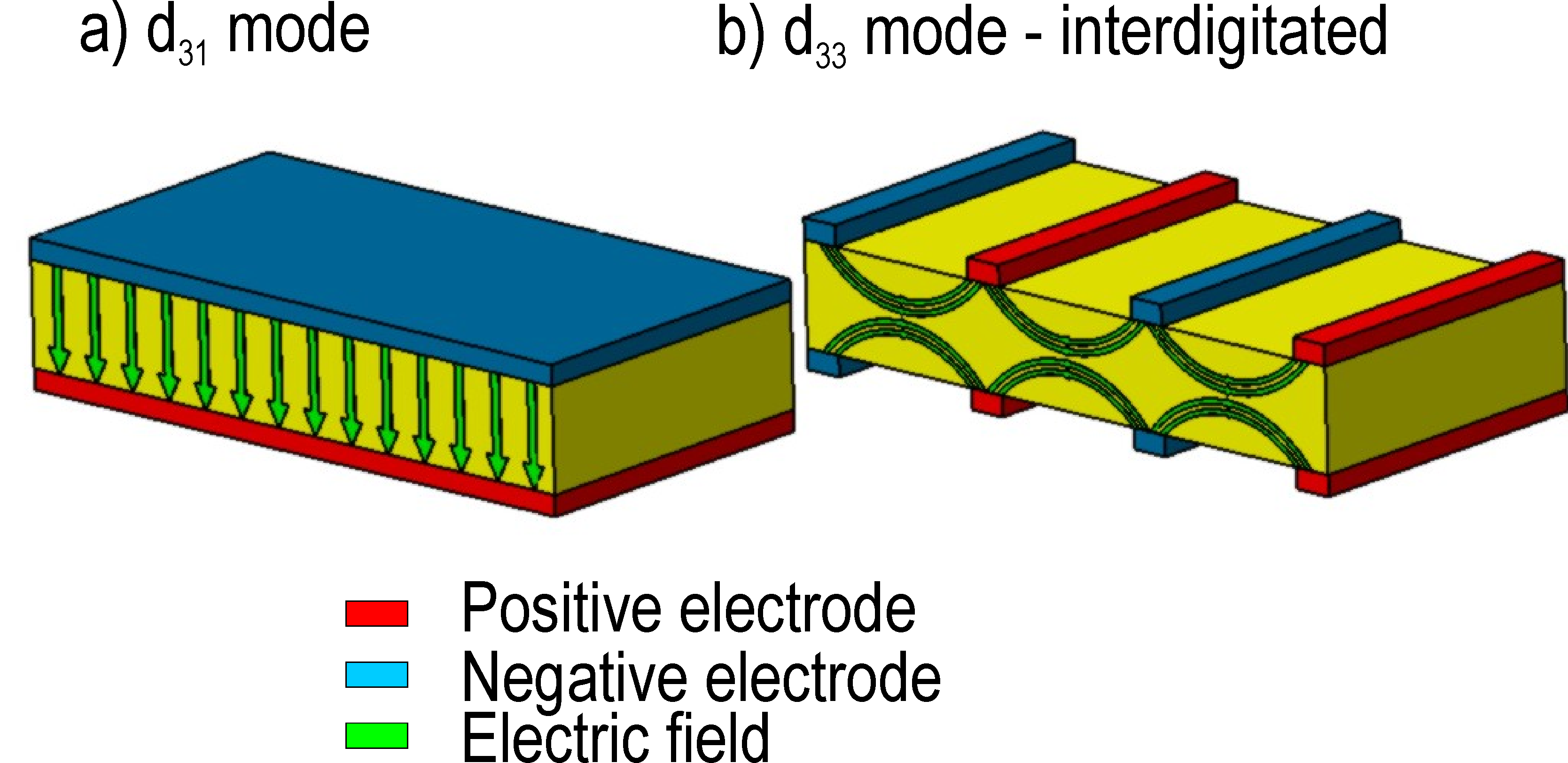
Figure 2.47: Electric field for a) continuous electrodes b) Inter-digitated electrodes
The behavior of a piezoelectric patch with interdigitated electrodes can be studied by considering a representative volume element as shown in Fig 2.48.
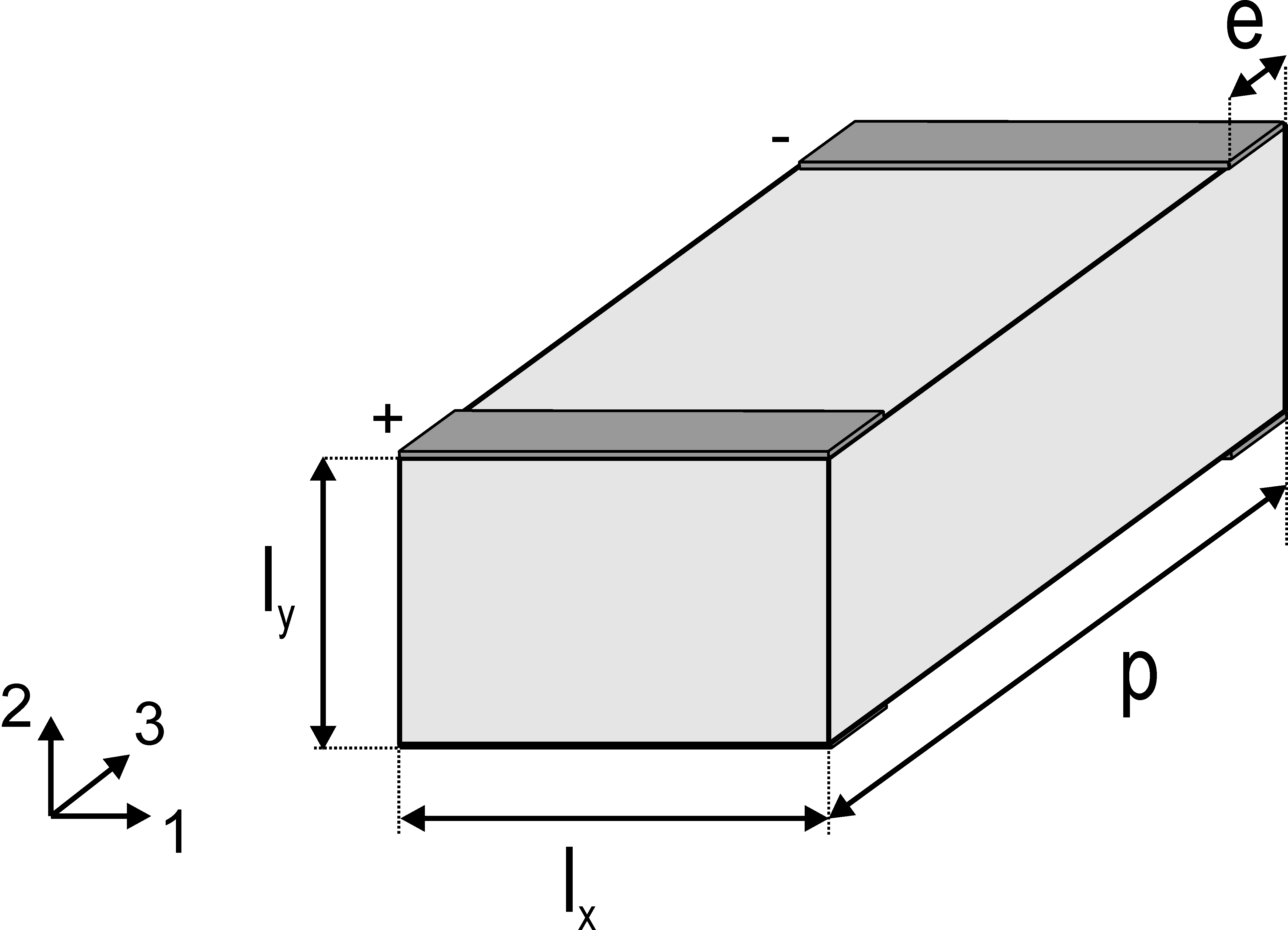
Figure 2.48: Definition of a representative volume element to study the behavior of a piezoelectric patch with IDEs
Let us consider such a piezoelectric patch whose geometrical properties are given in Table 2.7. The default material considered is again SONOX_P502_iso (Table 2.6).
Property Value lx 0.4 mm ly 0.3 mm p 0.7 mm e 0.05 mm
Table 2.7: Geometrical properties of the piezoelectric patch
We compute the static response due to a unit voltage applied across the electrodes, and represent the curved electric field:
( d_piezo('TutoPatch_num_IDE-s1')
). The mesh is first built in SI unit, and then transformed in mm.
d_piezo('TutoPatch_num_IDE-s1')
). The mesh is first built in SI unit, and then transformed in mm.
% See full example as MATLAB code in d_piezo('ScriptTutoIdePatch')
%% Step 1 - Build mesh
% Meshing script can be viewed with sdtweb d_piezo('MeshIDEPatch')
% Build mesh, electrodes and actuation
model=d_piezo(['MeshIDEPatch nx=10 ny=5 nz=14 lx=400e-6' ...
 'ly=300e-6 p0=700e-6 e0=50e-6']);
% Transform in mm
model.Node(:,5:7)=model.Node(:,5:7)*1000; % From m to mm
model.unit='mm';
% Convert material properties
model.pl = fe_mat('convert SI mm',model.pl);
(d_piezo('TutoPatch_num_IDE-s2')
)
%% Step 2 - Compute response due to V and visualize
% low freq response to avoid rigid body modes
model=fe_case(model,'pcond','Piezo','d_piezo(''Pcond'')');
model=stack_set(model,'info','Freq',10);
def=fe_simul('dfrf',model);
% Plot deformed shape
cf=feplot(model,def); fecom('view3'); fecom('viewy-90'); fecom('viewz+90')
fecom('undef line'); fecom('triax') ; iimouse('zoom reset')
(d_piezo('TutoPatch_num_IDE-s3')
)
%% Step 3 - visualize electric field
cf.sel(1)={'groupall','colorface none -facealpha0 -edgealpha.1'};
p_piezo('viewElec EltSel "matid1" DefLen 50e-3 reset',cf);
fecom('scd 1e-10')
p_piezo('electrodeview -fw',cf); % to see the electrodes on the mesh
iimouse('zoom reset')
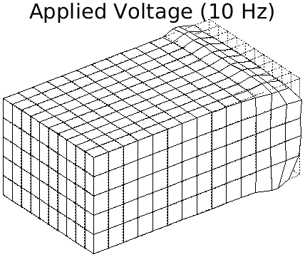
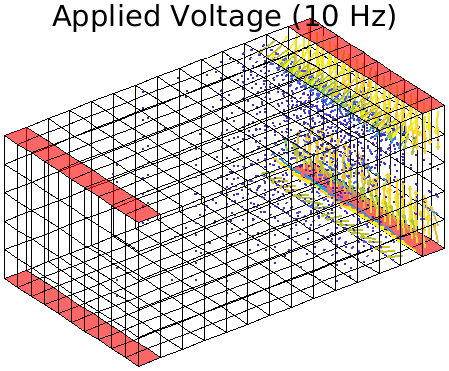
The resulting deformation and electric field are represented in Fig 2.49. The mean strains S1,S2 and S3 and the mean electric field in direction 3 (poling direction) are then computed. In this example, the electric field is aligned with the poling direction, but is of opposite direction, resulting in a negative value of the mean strain S3 (d33 is positive). Because d31 and d32 are negative, the mean values of S1 and S2 are positive: when the patch contracts in direction 3, it is elongated in directions 1 and 2. By dividing the mean strains by the mean electric field in the poling direction, one should recover the d31,d32 and d33 coefficients of the material. The mean value of E3 is however different from the value which would be obtained if the electric field was uniform (continuous electrodes on the sides of the patch). This value is considered here as the reference analytical value given by E3 = V/p. Note that due to the conversion to mm, the voltage is expressed in µ V.
a) b)
c)
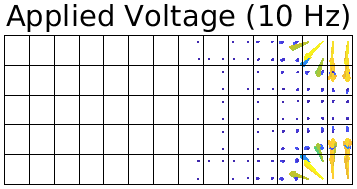
Figure 2.49: a) Free deformation of the IDE patch under unit voltage actuation b) 3D Electric field distribution and c) 2D Electric field
(d_piezo('TutoPatch_num_IDE-s4')
)
%% Step 4 - Compare efective values of constitutive law
% Decompose constitutive law
CC=p_piezo('viewdd -struct',cf); %
% Compute mean value of fields and deduce equivalent d_ij
% Uniform field is assumed for analytical values
a=p_piezo('viewstrain -curve -mean',cf); % mean value of S1-6 and E1-3
fprintf('Relation between mean strain on free structure and d_3i\n');
E3=a.Y(9,1); disp({'E3 mean' a.Y(9,1) -1/700e-3 'E3 analytic'})
disp([{'Sx/E3';'Sy/E3';'Sz/E3'} num2cell([a.Y(1:3,1)/E3 CC.d(3,1:3)']) ...
{'d_31(mm/muV)';'d_32(mm/muV)';'d_33(mm/muV)'}])
The ratio between the mean of E3 and the analytical value is about 0.80, which means that the free strain of an IDE patch with the geometrical properties considered in this example will be about 20 % lower than if the electric field was uniform. In fact, the spacing of the electrodes in an IDE patch is a compromise between the loss of performance due to the part of the piezoelectric material in which the electric field is not aligned with the poling direction, and the distance between the electrodes which, when increased, decreases the effective electric field for a given applied voltage. The total charge on the electrodes and the charge density are then computed.
(d_piezo('TutoPatch_num_IDE-s5')
)
%% Step 5 - Charge visualisation and total on electrodes
p_piezo('electrodeTotal',cf)
% charge density on the electrodes
feplot(model,def);
cut=p_piezo('electrodeviewcharge',cf,struct('EltSel','matid 1'));
fecom('view3'); fecom('viewy-90'); fecom('viewz+90'); iimouse('zoom reset');
iimouse('trans2d 0 0 0 1.6 1.6 1.6')
Figure 2.50 shows the distribution of the charge density on the electrodes.
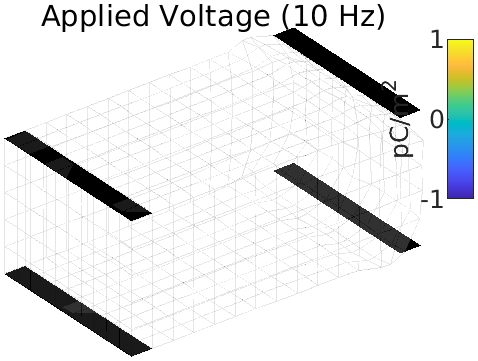
Figure 2.50: Charge density on the electrodes resulting from a static unit voltage applied to the IDEs
The capacitance of the patch can be computed and compared to the analytical value (for a uniform field) given by CT = єT (lx ly)/p:
(d_piezo('TutoPatch_num_IDE-s6')
)
%% Step 6 - Theoretical capacitance for uniform field
Ct=model.pl(1,22)*400e-3*300e-3/700e-3;
% total charge on the electrodes = capacitance (1 muV actuation)
C=p_piezo('electrodeTotal',cf);
% Differences are due to non-uniform field, this is to be expected
disp({'C_{IDE}' cell2mat(C(2,2)) Ct 'C analytic'})
The capacitance of the IDE patch is about 10% lower than the analytical value.
It is also interesting to plot color maps of strain and stress components in the patch , which can be done using fe_stress .
(d_piezo('TutoPatch_num_IDE-s7')
)
%% Step 7 - Stress  visualisation
% Stress field using fe_stress
c1=fe_stress('stressAtInteg -gstate',model,def);
cf.sel='reset';cf.def=fe_stress('expand',model,c1);
cf.def.lab={'T11';'T22';'T33';'T23';'T13';'T12';'D1';'D2';'D3'}; %
fecom('colordata 99 -edgealpha.1');
fecom('colorbar',d_imw('get','CbTR','String','Stress/Voltage [kPa/muV]'));
iimouse('trans2d 0 0 0 1.6 1.6 1.6')
Figure 2.51 shows the colormap of T1, T2 and T3. It is clear that the curved electrical field induces important stress concentrations in the area close to the electrodes
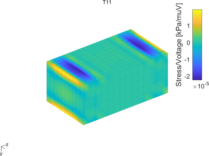
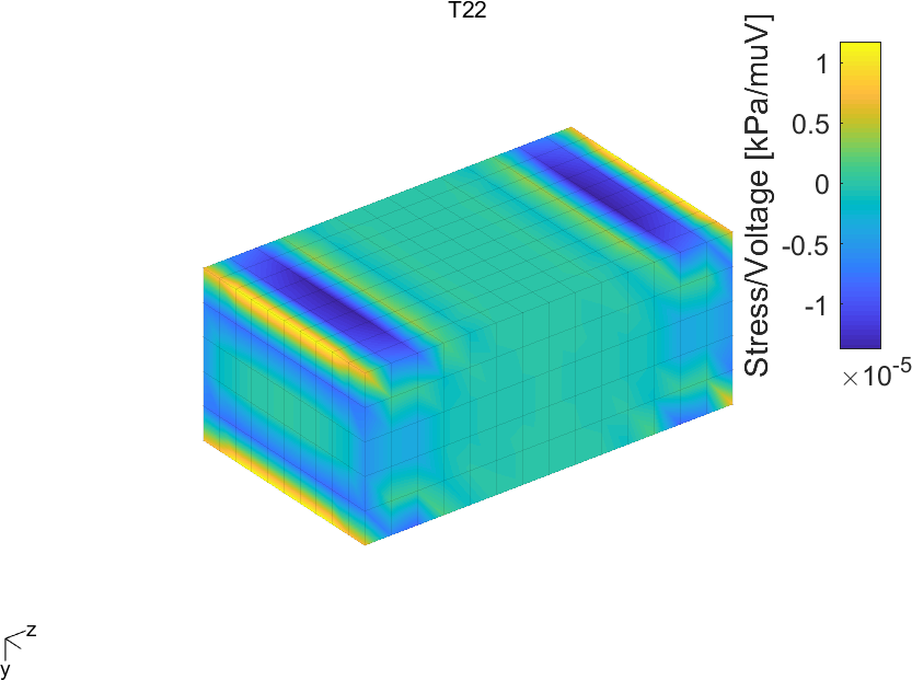
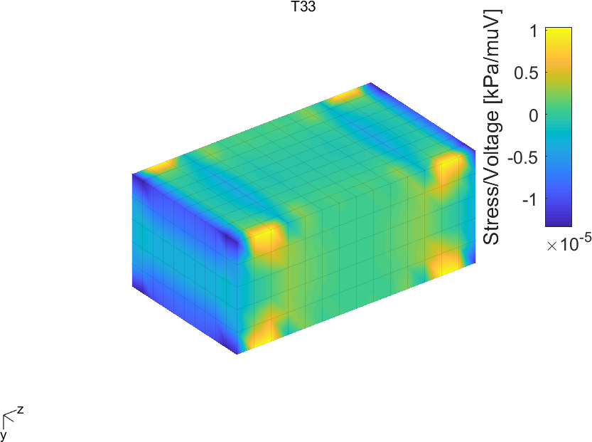
Figure 2.51: Colormap of stresses T1, T2 and T3 due to applied voltage on the patch with IDE
The strains and electrical displacement can also be computed with fe_stress , but this requires to replace the piezoelectric material with a 'PiezoStrain' material:
%% Step 8 - Strain  visualisation
% Replace with 'PiezoStrain' material
mo2=model; mo2.pl=m_piezo('dbval 1 PiezoStrain')
% Now represent strain fields using fe_stress
c1=fe_stress('stressAtInteg -gstate',mo2,def);
cf.sel='reset';cf.def=fe_stress('expand',mo2,c1);
cf.def.lab={'S11';'S22';'S33';'S23';'S13';'S12';'E1';'E2';'E3'};
fecom('colordata 99 -edgealpha.1');
fecom('colorbar',d_imw('get','CbTR','String','Strain/Voltage [1/muV]'));
iimouse('trans2d 0 0 0 1.6 1.6 1.6')
Figure 2.52 shows the colormap of S1, S2 and S3. The strain is uniform in the central regio, but there are strong variations in the areas under the electrodes
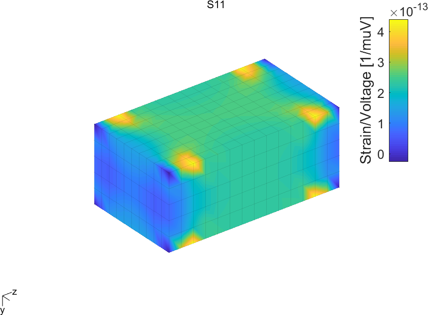
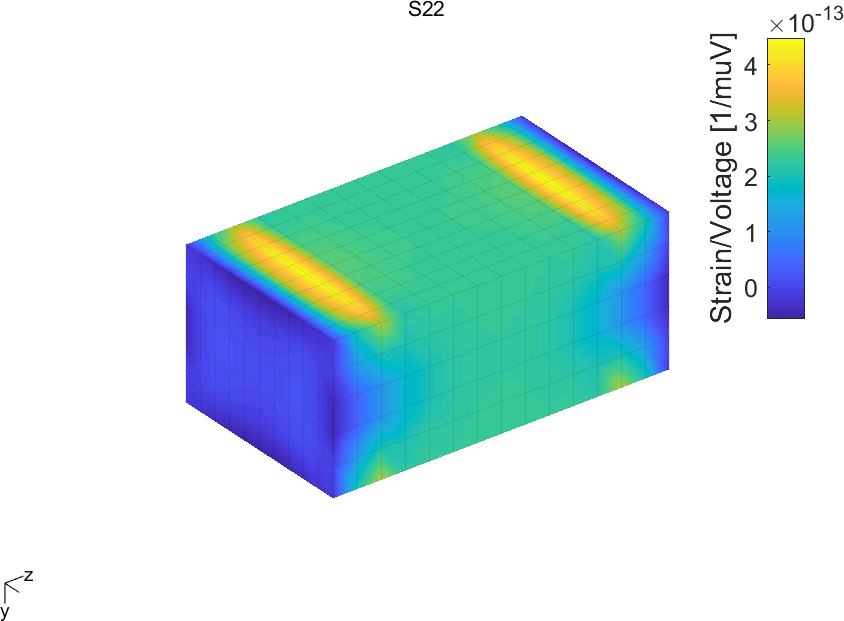
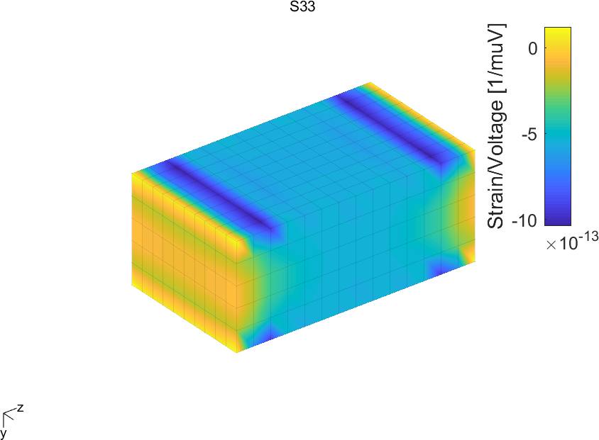
Figure 2.52: Colormap of strains S1, S2 and S3 due to applied voltage on the patch with IDE
Note that in this example, the poling direction has been considered to be aligned with the z-axis. In practice, as the IDE patch is usually poled using the IDE electrodes, the poling direction is aligned with the curved electric field lines. This difference of poling only concerns a few elements in the mesh, and from a global point of view, it does not have an important impact on the assessment of the performance of the patch, but it may have an important impact on the prediction of strains and stresses around the electrode areas. Aligning the poling direction with the curved electric field lines is possible but requires the handling of local basis which are oriented based on the computed electric field lines.

