PDF Index
| SDT-piezo
Contents
Functions
PDF Index |
2. Basics of piezoelectricity
Polarization consists in the separation of positive and negative electric charges at different ends of the dielectric material on the application of an external electric field (Figure 2.1).
Spontaneous polarization is the phenomenon by which polarization appears without the application of an external electric field. Spontaneous polarization has been observed in certain crystals in which the centers of positive and negative charges do not coincide. Spontaneous polarization can occur more easily in perovskite crystal structures.
The level and direction of the polarization is described by the electric displacement vector D:
| (1) |
where P is the permanent polarization which is retained even in the absence of an external electric field, and є E represents the polarization induced by an applied electric field. є is the dielectric permittivity. If no spontaneous polarization exists in the material, the process through which permanent polarization is induced in a material is known as poling.
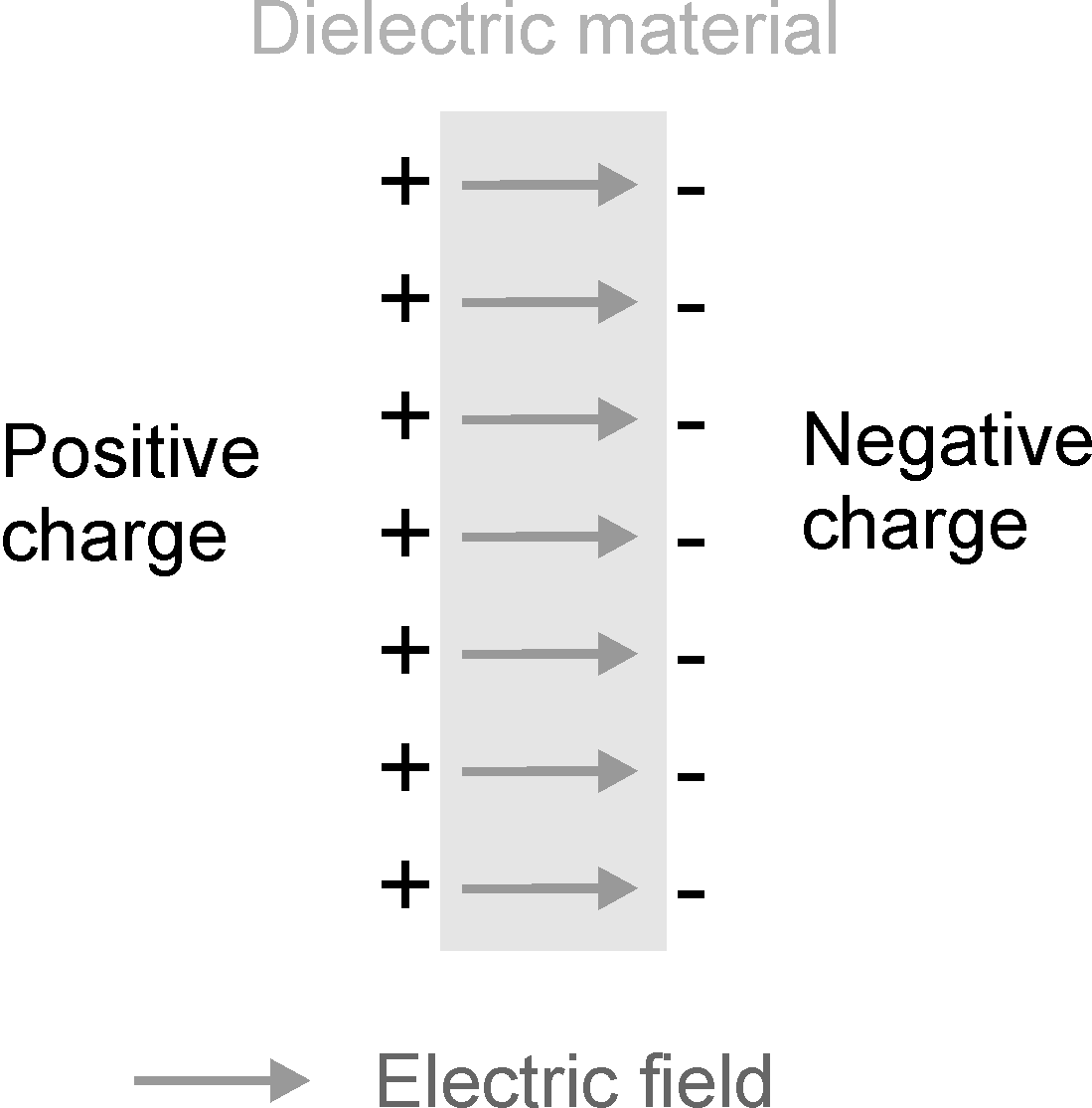
Figure 2.1: Polarization: separation of positive and negative electric charges on the two sides of a dielectric material
Ferroelectric materials have permanent polarization that can be altered by the application of an external electric field, which corresponds to poling of the material. As an example, perovskite structures are ferroelectric below the Curie temperature. In the ferroelectric phase, polarization can therefore be induced by the application of a (large) electric field.
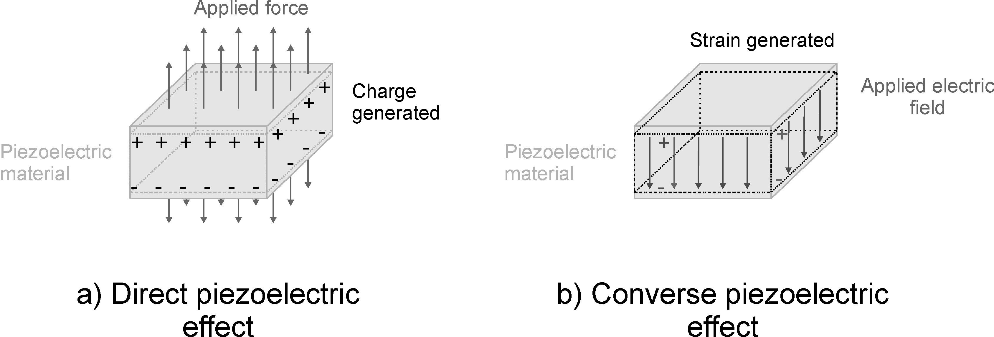
Piezoelectricity was discovered by Pierre and Jacques Curie in 1880. The direct piezoelectric effect is the property of a material to display electric charge on its surface under the application of an external mechanical stress (i.e. to change its polarization). (Figure 2.2a).
The converse piezoelectric effect is the production of a mechanical strain due to a change in polarization (Figure 2.2b).
Piezoelectricity occurs naturally in non ferroelectric single crystals such as quartz, but the effect is not very strong, although it is very stable.
The direct effect is due to a distortion of the crystal lattice caused by the applied mechanical stress resulting in the appearance of electrical dipoles. Conversely, an electric field applied to the crystal causes a distortion of the lattice resulting in an induced mechanical strain. In other materials, piezoelectricity can be induced through poling. This can be achieved in ferroelectric crystals, ceramics or polymers.
A piezoelectric ceramic is produced by pressing ferroelectric material grains (typically a few micrometers in diameter) together. During fabrication, the ceramic powder is heated (sintering process) above Curie temperature. As it cools down, the perovskite ceramic undergoes phase transformation from the paraelectric state to the ferroelectric state, resulting in the formation of randomly oriented ferroelectric domains. These domains are arranged in grains, containing either 90∘ or 180∘ domains (Figure 2.3a). This random orientation leads to zero (or negligible) net polarization and piezoelectric coefficients (Figure 2.3b)).
a) b)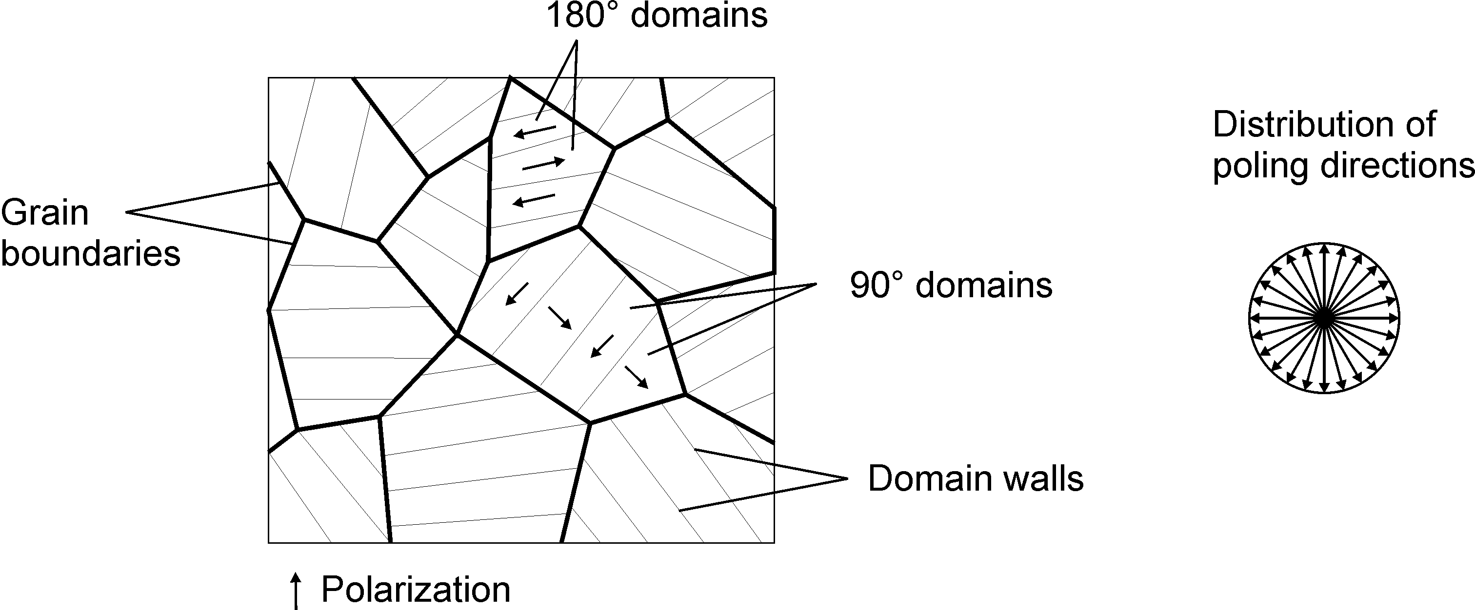
Figure 2.3: Piezoelectric ceramic : a) ferroelectric grains and domains, b) distribution of poling directions
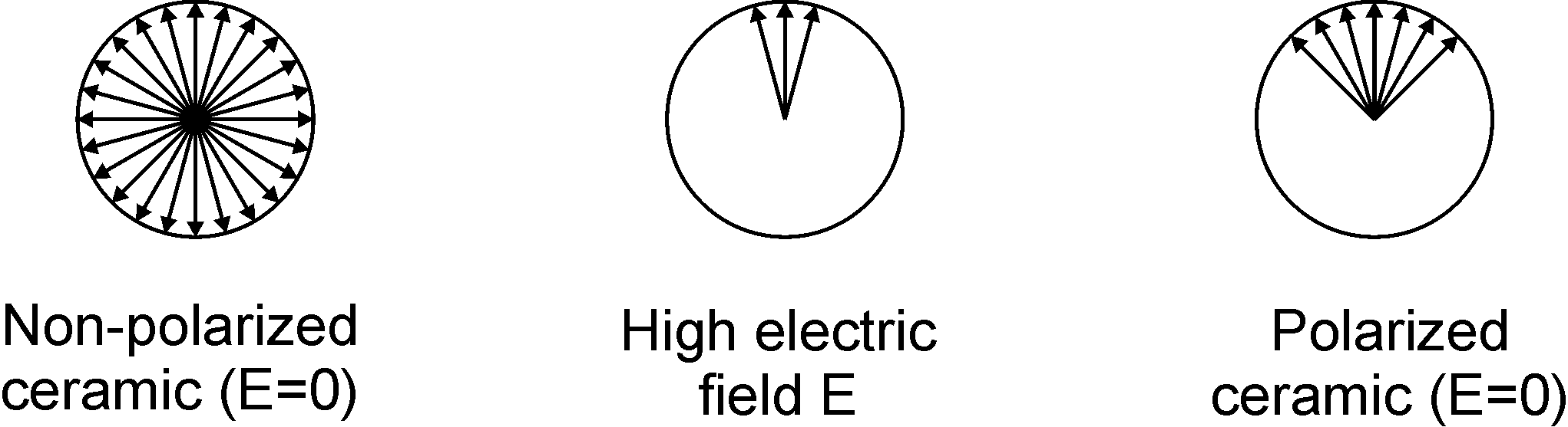
The application of a sufficiently high electric field to the ceramic causes the domains to reorient in the direction of the applied electric field. Note however that the mobility of the domains is not such that all domains are perfectly aligned in the poling direction, but the total net polarization increases with the magnitude of the electric field (Figure 2.4). After removal of the applied electric field, the ferroelectric domains do not return in their initial orientation and a permanent polarization remains in the direction of the applied electric field (the poling direction). In this state, the application of a moderate electric field results in domain motions which are responsible for a deformation of the ceramic and are the source of the piezoelectric effect.
The poling direction is therefore a very important material property of piezoelectric materials and needs to be known for a proper modeling.
Typical examples of simple perovskites are Barium titanate (BaTiO3) and lead titanate (PbTiO3). The most common perovskite alloy is lead zirconate titanate (PZT- PbZr TiO3). Nowadays, the most common ceramic used in piezoelectric structures for structural dynamics applications (active control, shape control, structural health monitoring) is PZT, which will be used extensively in the documented examples.
In certain polymers, piezoelectricity can be obtained by orienting the molecular dipoles within the polymer chain. Similarly to the ferroelectric domains in ceramics, in the natural state, the molecular dipole moments usually cancel each other resulting in an almost zero macroscopic dipole. Poling of the polymer is usually performed by stretching the polymer and applying a very high electric field, which causes the molecular dipoles to orient with the electric field, and remain orientated in this preferential direction after removal of the electric field (permanent polarization). This gives rise to piezoelectricity in the polymer. The technology of piezoelectric polymers has been largely dominated by ferroelectric polymers from the polyvinylidene fluoride (PVDF) family, discovered in 1969. The main advantage is the good flexibility, but their piezoelectric coefficients are much lower compared to ferroelectric ceramics.